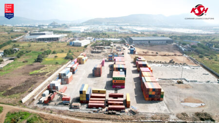
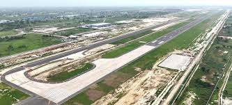
A 20-member Japanese team visited Dholera SIR to assess opportunities in semiconductor manufacturing and infrastructure.
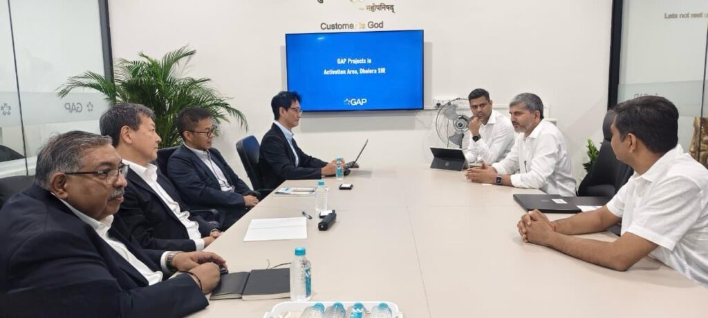
A high-level Japanese delegation comprising 20 semiconductor ecosystem companies toured Dholera Special Investment Region (SIR) this week to explore avenues for collaboration. The group included senior executives from Shimizu Corporation, a major name in infrastructure and precision engineering.
The visit followed SEMICON India 2025, where India highlighted its policy framework and fiscal incentives for chip production. At Dholera’s ABCD Building, discussions were held between Shimizu representatives and GAP Group, a regional developer, on leveraging Japanese precision technology with India’s scale, workforce, and robust infrastructure.
Talks focused on developing precision facilities for Japanese SMEs that would support Tata Semiconductor and other fabrication plants in the region. Plans also included building warehouses, gas distribution networks, clean rooms, as well as residential and hospitality projects for engineers and managers. Skill development initiatives in semiconductor manufacturing were also discussed.
Dholera already houses India’s largest semiconductor fabrication facility, a Tata Group–PSMC joint venture worth ₹92,000 crore, expected to commence production by 2027 and generate thousands of jobs.
Source: PR


